- Home
- Products
- News
- About Us
- Support center
- Contact Us
inquiry
Leave Your Message
You know, in the fast-paced world of electronics manufacturing, making sure circuit boards are top-notch and reliable is super important. For a long time, folks have turned to Circuit Board X-Ray Machines to spot defects and keep things running smoothly. But with technology constantly moving forward, manufacturers and engineers are starting to check out other options that might even give them better results. In this blog, we’re going to dive into some of the best alternatives to those X-Ray machines, shining a light on some cool methods and solutions that are really picking up steam in the industry.
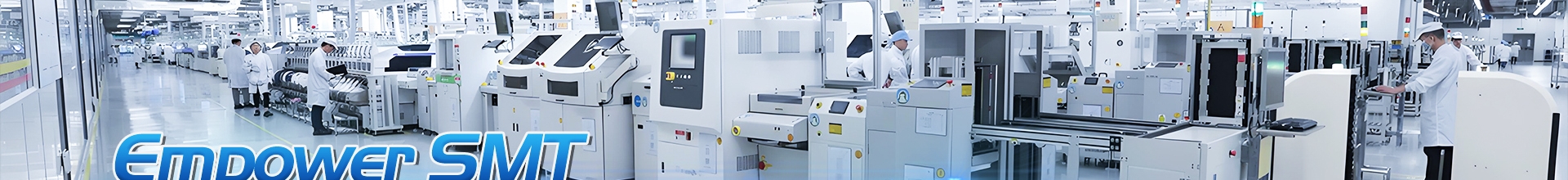
At Morel Equipments Co., Limited, we’re all about being your one-stop shop in the surface mount technology (SMT) game, and we’ve been at it for over 15 years now! Our journey has not just let us provide some seriously high-quality accessories, but we’ve also developed some pretty advanced gear like Pick And Place Machines, automatic soldering robots, and ICT & FCT automatic testers. As we take a closer look at these alternatives to Circuit Board X-Ray Machines, we’re hoping to share insights that can help manufacturers really boost their quality assurance processes and overall production efficiency.

So, X-ray machines have really become a must-have in the whole circuit board inspection game. They give us some seriously valuable insights into what's going on inside those electronic components. You know, they can uncover hidden defects—like those tricky solder joints that you just can't spot from the outside. That’s super important for making sure our devices work reliably and last longer. These machines are equipped with some pretty advanced imaging techniques that help us catch issues like voids, cracks, or misalignments that could really mess things up. And get this, the technology behind X-ray inspection just keeps getting better! We’re talking clearer images and quicker processing times. Because of this, manufacturers definitely need to include these machines in their quality control processes. With all these tiny components and complex designs nowadays, the demand for precise inspection methods has never been higher. X-ray machines can even handle multilayer circuit boards, giving us insights that traditional methods—like just looking at stuff or using automated optical inspection—might totally miss. Now, while X-ray machines are absolutely invaluable, it might also be worth it to look into some alternative inspection techniques that can either add to what X-rays do or even take their place in some situations. Techniques like acoustic microscopy or micro-CT scanning can definitely give us a different look at how solid a circuit board is. These alternatives might come with benefits like lower costs or fewer safety worries, and they offer some unique advantages in specific cases. It’s all about enriching the toolset engineers and manufacturers have as they navigate the ever-evolving world of electronics!

Circuit board X-ray machines have become a staple for quality assurance in the electronics industry, but they come with significant limitations that manufacturers must consider. One of the key issues is the challenge of detecting specific failure mechanisms, such as conductive anodic filament (CAF) defects. Recent studies, including a root cause analysis of a PCB failure in a public transportation communication system, highlighted that even CAF-resistant PCBs can fall victim to this failure mode due to PCB de-penalization. This indicates that reliance solely on X-ray inspection may not identify faults that arise from complex material interactions, particularly in environments prone to conductive pathways.
Moreover, the efficacy of X-ray machines in detecting hidden flaws is often hampered by the increasing complexity of PCB designs. As circuit boards become more intricate, traditional X-ray machines may struggle to provide clear insights into inner layer connections or errors that may arise from outsourcing vulnerabilities in the PCB supply chain. Recent data reports underscore that this outsourcing can lead to malicious activities, altering the integrity of PCB components globally. These factors highlight the critical need for alternative inspection methods that enhance defect detection and ensure the reliability of circuit boards.
Additionally, as industries pivot towards smarter technology integrations, the limitations of X-ray machines may hinder their capability in meeting stringent new safety and performance standards. The fusion of information technology with operational technology can offer enhanced data utilization, suggesting a shift towards more integrated inspection solutions that leverage real-time data analytics rather than solely relying on traditional methods like X-ray imaging.

So, when we talk about non-destructive testing (NDT) methods for analyzing PCBs, it’s pretty cool to see that alternatives to the old-school X-ray machines are really starting to pick up steam. One of the exciting new approaches is using 3D printed devices tailored for specific jobs, like the Impact Echo method, which is actually used for detecting cracks in concrete. This DIY tool really highlights how modern manufacturing techniques can be cleverly adapted to create handy gadgets for checking structural integrity, and it gets folks thinking about similar solutions for PCB inspections.
But wait, there’s more! Beyond these impact echo techniques, there have been some neat advancements in electromagnetic methods, especially with coplanar rectangular spiral coils. Researchers have come up with some solid analytical models to figure out the mutual inductance between these coils, which makes it possible to inspect printed circuit boards without causing any harm. These methods actually take advantage of changes in magnetic flux to give us a peek inside the structure and help identify faults—all without putting those sensitive components at risk.
By mixing it up with different NDT methods, engineers and technicians can really fine-tune the inspection process to meet the unique needs of their PCB projects. Exploring these alternatives not only boosts the reliability of testing but also sparks innovation within the industry, pushing the limits of what we can achieve in electronic circuit analysis.

You know, when it comes to checking circuit boards, optical inspection systems are really shaking things up and proving to be a much better option than the old-school X-ray machines. One of the biggest perks? Speed! Just take a look at what Saki Corporation has rolled out – they've developed the fastest 3D Automated Optical Inspection Machine. It can quickly go through complex circuit board designs while still being super accurate. This quick turnaround is a game changer in today’s manufacturing world, especially when getting products to market quickly is everything.
And there’s more! These optical inspection systems are powered by some seriously advanced AI technology. This means they're able to spot tiny defects that could end up jeopardizing the circuit boards' integrity. With their smart algorithms, they can analyze connections, pads, and traces like never before. Plus, thanks to deep learning frameworks, they can swiftly classify any manufacturing defects. This really boosts quality control, making sure the electronic components produced are reliable and top-notch.
What’s really cool is how optical inspection fits right into the smart manufacturing trend. For example, those clever assembly process improvement systems can take feedback from inspections to tweak production strategies on the fly. This kind of integration promotes continuous improvement, which helps cut down on defects and makes the best use of resources. As manufacturers work to up their reliability and efficiency, optical inspection systems are definitely standing out as a crucial piece in the puzzle of enhancing circuit board quality assurance.
You know, as technology keeps advancing, figuring out better ways to inspect electronics is more crucial than ever. Take circuit board X-ray machines, for instance—they’ve been around forever and are a big part of quality control. But there are some cool new automated inspection methods popping up that could give them a run for their money. These innovations not only bring different ways to check things but also step up the game in terms of efficiency and accuracy when it comes to spotting defects.
Let’s talk about one exciting option: Automated Optical Inspection, or AOI for short. This tech uses high-resolution cameras paired with really smart software to scrutinize printed circuit boards (PCBs) for any surface defects, misalignments, or other hiccups. What’s awesome about AOI is that it can analyze things in real-time and provide quick feedback, which is totally essential for busy production lines that need to keep up quality while cranking out products. Plus, the way it allows for speedy adjustments based on its findings makes it a fantastic sidekick to X-ray inspections, especially for problems that are easy to see on the surface.
Then we've got Laser Fault Detection, which is pretty nifty too. This technique uses lasers to scan the surfaces and edges of those circuit boards, spotting discrepancies with laser-like precision—pun intended! The beauty of this method is that it's non-destructive. That means manufacturers can inspect components without risking damage to their physical parts. And hey, when you mix laser systems with AI-driven analytics, it really amps up defect recognition, turning it into a cutting-edge solution for automated inspection.
And let's not forget about Thermal Imaging, which is really starting to catch on as a handy tool for inspecting circuit boards. By looking at heat patterns, it can reveal hidden defects linked to electrical connections, soldering quality, and component performance. As circuits do their thing, any weird temperature spikes can hint at potential failures, so catching those early on helps avoid major disasters. In this sense, thermal imaging turns into a powerful ally in the toolbox of automated inspection technologies.
You know, when it comes to finding effective ways to inspect stuff across different industries, there's a lot of buzz about how computed tomography (CT) scanning stacks up against the classic X-ray inspection. X-ray has been the go-to method for non-destructive testing for ages, but now that CT scanning's in the picture, it's really stepping up the game by offering way more detail about what's happening inside structures.
So, here’s the cool part: CT scanning uses some fancy algorithms to take a bunch of 2D X-ray images and stitch them together into 3D models. This means better spatial resolution and a chance to see those intricate shapes that used to be so tricky to visualize. It’s a game-changer, especially in fields like biomedical imaging, where high resolution is not just a bonus, it’s essential. Plus, have you heard about the latest innovations in dynamic X-ray imaging? We’re talking about screen-printed perovskite CMOS arrays that really kick things up a notch, improving both how finely we can see things and how fast.
These advancements are pretty exciting—they show that CT scanning isn’t just keeping pace with traditional X-ray methods; in some cases, it’s actually taking the lead by providing a richer, more detailed look at the diagnostics we need.
And let’s face it, as industries keep bringing in newer, high-tech materials, nailing radiographic testing and industrial CT is becoming more important than ever. With these high-tech imaging systems, we can really dive deep into understanding different components and figure out potential failure points—this definitely ups the game for quality assurance. As businesses start leaning towards these cutting-edge alternatives, I can’t help but think the conversation about CT versus X-ray inspection is bound to get even more interesting, especially with the growing push for accuracy and efficiency in inspection practices.
You know, ultrasound testing has really become a solid option for checking out the quality of circuit boards, especially in places where the usual X-ray inspections just don’t cut it. Recently, we’ve seen some pretty cool advancements in ultrasound tech, like robotic systems that can adjust in real-time based on what they’re seeing. This not only makes things quicker but also safer during inspections, which is awesome for reducing risks related to contact and exposure. It’s interesting to see how these innovations mirror what’s happening in other medical areas. Take, for instance, that fully autonomous robotic ultrasound system that’s been developed for scanning thyroids—it's a great reminder of how critical expertise is for getting top-notch images.
The whole ultrasound thing in non-destructive testing (NDT) isn’t just a fad, either; there’s tons of research backing it up. It’s especially good at uncovering defects in materials like carbon fiber-reinforced polymers. There was even a study in the Journal of Sensors that highlighted just how important ultrasonic testing can be in industries that rely on composite materials. One of the best things about ultrasound tech is its flexibility— it lets us check out different structures without risking damage, which is super important when it comes to circuit boards.
And it gets even better! With advanced image quality metrics coming from linear system theory, ultrasound imaging has gotten way more reliable. This means we can classify and assess image quality better, which is key to spotting any potential failures in electronic components. By using high-frequency ultrasonic transducers, industries can really step up their inspection game, making sure they keep those high standards in circuit board production and overall quality assurance.
You know, visual inspection techniques have really taken off lately as some pretty smart alternatives to those pricey circuit board X-ray machines. A report from IPC in 2021 hinted that around 70% of companies are jumping on the bandwagon with these visual methods because, let's face it, they're more affordable and efficient. These techniques not only help companies save a pretty penny on capital investments but also cut down on those ongoing costs for maintenance and calibration that come with the fancy X-ray systems.
One standout method in the visual inspection realm is Automated Optical Inspection, or AOI for short. According to a study from ECIA in 2020, these AOI systems can catch defects at a rate of over 95%, which is not far off from what traditional X-ray inspections can do, especially for things like solder joints and component placements. It's pretty cool how this method uses high-res cameras and advanced algorithms to spot any weirdness in the manufacturing process, making quality control a lot better.
And let's not forget about good old manual inspection. It's definitely still a valid option, particularly for smaller production runs or prototypes. A 2022 report from EETimes pointed out that while manual inspection might not be as accurate, it gives you real-time feedback and the chance to tweak things on the fly, which can really boost product quality. The flexibility that visual inspection techniques offer is super attractive for businesses trying to strike that sweet balance between cost and precision in the fast-paced electronics market.
Alternatives include the Impact Echo method using 3D printed devices, electromagnetic methods with coplanar rectangular spiral coils, and advancements in automated inspection technologies like Automated Optical Inspection (AOI), Laser Fault Detection, and Thermal Imaging.
The Impact Echo method uses 3D printed devices to detect cracks and structural integrity in materials, which can be applied in diagnosing issues within printed circuit boards without causing damage.
AOI utilizes high-resolution cameras and software to detect surface defects and misalignments on PCBs, enabling real-time feedback and adjustment for quality control in production lines.
Laser Fault Detection scans boards with high precision without damaging them, and it can be enhanced with AI analytics to improve defect recognition and inspection efficiency.
Thermal Imaging analyzes heat patterns to identify potential defects related to electrical connections and component functionality, allowing manufacturers to intervene before failing components can cause serious issues.
Diversifying NDT methods allows engineers to tailor inspection processes to specific project needs, enhancing reliability and promoting innovation in electronic circuit analysis.