- Home
- Products
- News
- About Us
- Support center
- Contact Us
inquiry
Leave Your Message
The world of Printed Circuit Board (PCB)technology is evolving at a pretty rapid pace right now, and Pcb Routers are really leading the charge with these innovations. It’s hard to ignore how the global market for PCBs is expected to hit a whoppingUSD 72.3 billion by 2025 — and a big part of that growth? The rising demand for small, powerful electronic gadgets. Because of that, having efficient routing tech is more crucial than ever.

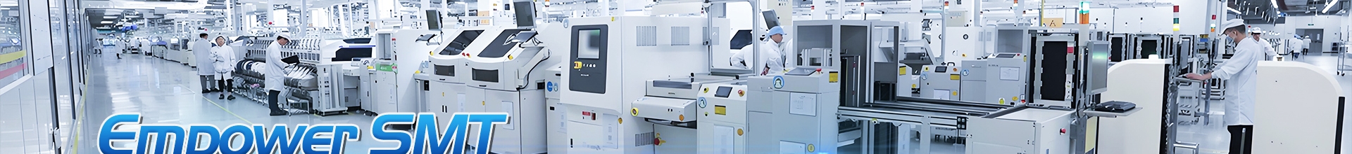
Now, let me tell you a bit about Morel Equipments Co., Limited. They’ve been in the surface mount technology (SMT) game for over 15 years, and they’ve really made a name for themselves as a one-stop shop. They offer top-of-the-line gear like pick-and-place machines, automatic soldering robots, and solder paste equipment. In this piece, I want to dive into some of the latest trends and innovations shaping PCB router tech. You’ll see how advances in automation and precision are totally transforming manufacturing — boosting productivity and changing the game for the electronics industry.
The world of PCB router technology is changing pretty quickly these days, thanks to some exciting new tech that's really shaking up how we do things. One of the coolest developments has to be the way AI and machine learning are being integrated. These smart systems can look at your design patterns and kinda predict the best routing paths, which means less time wasted and fewer mistakes — saving both money and hassle in the long run. It’s like having a digital assistant helping you get it right the first time.
On top of that, additive manufacturing, like 3D printing, is becoming a game changer. It lets us create much more complex shapes and customizations that old-school subtractive methods just can't handle. Not only does this make miniaturization easier, but it also opens the door to combining multiple functions into one single board. That means smaller, more versatile devices—pretty awesome, right? As these tech trends keep evolving, they’re set to redefine industry standards and push the creative limits of PCB design and manufacturing.
The global laser marking market is increasingly transforming PCB manufacturing, enhancing precision and efficiency. As detailed in recent industry reports, the adoption of advanced laser marking technology is expected to grow at a compound annual growth rate (CAGR) of over 5% in the coming years due to rising demand for high-quality PCB applications in various sectors, including electronics and telecommunications. This growth highlights the significance of advanced features in laser marking machines, particularly the S-Series, which offer significant improvements in operational efficiency and marking accuracy.
The Direct Mounting Machine with Double Track, boasting a 686mm track width, exemplifies these advancements. Its independent engraving mode allows simultaneous operations on two tracks—enhancing productivity by enabling different engraving tasks to be executed concurrently. This capability is crucial in a landscape where rapid turnaround times are essential. With a doubling of the PCB size capacity to 450*250mm for double track configurations and a monorail setup accommodating sizes up to 450*450mm, manufacturers can achieve more versatile production capabilities, catering to diverse client needs while maintaining high-quality standards.
Moreover, the implementation of independent transmission boards significantly reduces transmission time to zero, ensuring that the workflow is not only streamlined but also highly efficient. As the global PCB manufacturing sector continues to evolve, incorporating such innovative laser marking solutions will be pivotal in maintaining a competitive edge, optimizing production processes, and meeting the precision demands of today's market. As such, embracing these technologies is not merely an option but a strategic necessity for manufacturers aiming to thrive in this dynamic industry.
: The main advancements include the integration of artificial intelligence (AI) and machine learning (ML) for improved routing algorithms, as well as the adoption of additive manufacturing techniques like 3D printing, allowing for more complex designs and functionalities.
AI and machine learning enhance routing algorithms by analyzing design patterns and predicting optimal routing paths, which significantly reduces time, costs, and errors in circuit board production.
Additive manufacturing, particularly 3D printing, allows for more intricate geometries and customizations in PCB designs, which facilitates miniaturization and the integration of multiple functionalities into a single board.
Automation in PCB routing is leading to faster production times, reduced human error, and increased output quality, with high-speed routers that can adjust parameters in real-time.
Robotics enhances PCB routing by performing intricate tasks with high accuracy, handling complex designs, and minimizing waste by optimizing routing paths to use material efficiently.
Manufacturers face challenges such as integrating advanced materials, achieving higher precision in routing processes, and maintaining cost efficiency while adapting to new technologies.
Morel Equipments Co., Limited is leveraging its experience in the surface mount technology industry to provide comprehensive solutions, including advanced products that enhance operational efficiency and accuracy in PCB production.
Future trends include continued advancements in automation and robotics, leading to enhanced scalability and flexibility in PCB production, as well as potentially new industry standards for design and fabrication.
Precision in PCB routing is crucial for the quality and reliability of circuit boards, as it minimizes errors, maximizes material usage, and ultimately contributes to the performance of electronic devices.
While integrating new technologies can pose challenges regarding cost efficiency, it ultimately aims to lower costs in the long term by reducing errors, improving production speeds, and enhancing overall quality.
So, it’s pretty exciting to see how PCB router tech is evolving lately. There are a bunch of new innovations and trends shaping its future. For instance, more and more, AI and machine learning are making their way into routing processes, which means those routers are becoming smarter and way more efficient—leading to more accurate designs. And it doesn't stop there. Sustainability is also a big deal now, pushing manufacturers to adopt more eco-friendly practices. Plus, the latest software tools are helping speed things up in PCB routing, making workflows smoother and more streamlined. Automation and robotics are taking things to the next level, promising faster production times without sacrificing precision.
That said, it’s not all smooth sailing. There are still some hurdles to overcome. Companies like Morel Equipments Co., Limited, with over 15 years of experience in surface mount tech, are right there in the thick of it. They’re really well-positioned to tap into these trends and push the envelope. By offering cutting-edge solutions like Pick And Place Machines and automatic soldering robots, Morel is leading the charge into this new era of PCB routing—embracing all the opportunities that come with these tech advancements.