In the fast-changing world of electronics manufacturing, quality control has honestly never been more important. You know, things like Solder Paste Inspection (SPI) really play a crucial role in making sure those connections on printed circuit boards (PCBs) are solid. It’s kinda shocking, but according to IPC-A-610, nearly 40% of PCB defects come down to crappy solder jobs. That really shows just how vital SPI is for avoiding production hiccups and those nasty reworks that can drain time and money.
And get this — the market for better SPI tech is booming, expected to hit around $2 billion by 2026. Industry giants like Koh Young and CyberOptics are pushing the envelope with smarter, more innovative inspection tools. That said, even the coolest machines can have their quirks — sometimes triggering false alarms or missing defects, which means operators still need to use their judgment. So, understanding the ins and outs of Solder Paste Inspection becomes essential if you wanna keep that quality bar high and production running smoothly.
Skip or skimp on a solid SPI process, and you risk serious fallout — think unexpected product failures once they’re out in the field. As electronics keep getting more complicated, manufacturers really need to take a good hard look at their inspection methods. Tackling these challenges head-on can seriously boost reliability and keep customers happy, especially in such a competitive landscape.

What is Solder Paste Inspection?
Solder paste inspection is a critical step in the electronics manufacturing process. This practice ensures that solder paste is applied correctly on printed circuit boards (PCBs). A Solder Paste Inspection Machine plays a vital role in this process by identifying issues early. Common problems include inconsistent solder paste volume and misalignment. These defects can lead to poor solder joints and affect the overall reliability of a device.
Using a Solder Paste Inspection Machine provides both speed and accuracy. It captures images of the solder paste deposits and analyzes them using sophisticated algorithms. The machine can detect discrepancies, helping manufacturers prevent potential failures.Failing to address these issues can result in costly rework and delayed production timelines.
However, relying solely on technology has its drawbacks. While inspection machines are precise, human oversight is essential. Operators must interpret the data properly. Addressing false positives created by the machine can be challenging. The interplay between automated systems and human experience is crucial for optimal results in solder paste inspection.
The Importance of Solder Paste Quality in Electronics Manufacturing
Solder paste quality plays a crucial role in electronics manufacturing. It directly affects the reliability and performance of printed circuit boards (PCBs). Poor solder paste quality can lead to defects in solder joints, risking device functionality. The process of Spi Solder Paste Inspection ensures that the right amount and consistency of solder paste are applied to each pad before components are placed. This step is essential for achieving high manufacturing standards.
Tips: Regular maintenance of inspection equipment is crucial. A well-calibrated system improves detection accuracy. Additionally, periodic training for operators helps keep inspection skills sharp. Training boosts confidence in making quick, informed decisions during production.
Variability in solder paste composition can create challenges. For example, different types of solder paste may require distinct handling and application techniques. Many manufacturers overlook these nuances. A thorough analysis of the paste, and its compatibility with other materials, is vital. In some cases, teams may need to revisit their processes to accommodate these differences, emphasizing a culture of continuous improvement.
Common Methods for Solder Paste Inspection
Solder Paste Inspection (SPI) is crucial in PCB manufacturing. It ensures that the solder paste application is correct. Incorrect application can lead to defects. According to IPC standards, 80% of assembly defects result from poor soldering processes. This emphasizes the need for effective inspection methods.
Common inspection methods for solder paste include automated optical inspection (AOI) and X-ray inspection. AOI uses cameras to detect solder paste shape and size. It instantly measures the paste height. Research shows that AOI can catch up to 98% of defects.
X-ray inspection, on the other hand, examines hidden solder joints. It is essential for BGA components. Approximately 30% of solder joint failures occur in concealed areas.
Each method has limitations. AOI can miss certain defects if the paste is correctly sized but poorly aligned. X-ray inspection is more time-consuming and costly. Understanding these nuances is vital for improving solder paste quality. Professionals must evaluate which method best fits their production lines to minimize risks effectively.
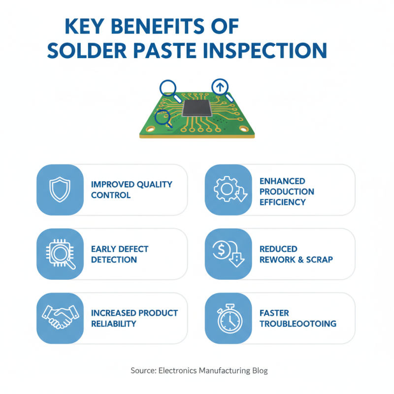
Key Benefits of Implementing Solder Paste Inspection
Solder Paste Inspection (SPI) is a crucial step in electronics manufacturing. It ensures quality control by verifying the correct application of solder paste on printed circuit boards (PCBs). Implementing SPI provides numerous benefits that enhance the overall production process.
One key benefit is defect detection. SPI helps identify issues like insufficient or excessive solder paste application. These defects can lead to poor connections or, worse, board failures. Identifying these problems early saves time and money, avoiding costly rework or product returns.
Another advantage is process optimization. By analyzing SPI data, manufacturers can fine-tune their Solder Paste Printing processes. This leads to improved consistency and reduces waste. However, some manufacturers may face challenges in analyzing data accurately, leading to flawed adjustments. It’s essential to invest time in training staff to interpret these results effectively. Technology can help, but human insight remains valuable.
Challenges in Solder Paste Inspection Processes
Solder paste inspection is an essential step in electronics manufacturing. It ensures that the amount of solder paste applied to the printed circuit board is consistent and accurate. However, several challenges complicate the Solder Paste Inspection Processes. One major issue is the variability in solder paste itself. Different formulations can behave uniquely during application. A report by IPC states that improper solder paste viscosity can lead to application defects.
Equipment also plays a significant role. Many machines struggle to provide consistent readings due to dust or environmental factors. These inconsistencies can cause false negatives or positives during inspections. According to a study from the Journal of Electronic Manufacturing, about 30% of inspections yield incorrect results that require rework, wasting both time and resources.
Tips: Regular calibration of inspection machines can mitigate inaccuracies. Additionally, ensuring that the work environment is clean can reduce contamination. Invest in training for operators to become proficient in recognizing common defects. This proactive approach can improve the overall efficiency of the solder paste inspection process and reduce errors.
Future Trends in Solder Paste Inspection Technology
Solder paste inspection technology is evolving rapidly. Innovations aim to enhance accuracy and efficiency. New forms of inspection leverage advanced algorithms and machine learning. These technologies help detect defects quickly and reliably. They promise to reduce manual inspection errors. However, the integration of such systems poses challenges. Training personnel to operate these systems effectively can be difficult.
Moreover, the move towards automation in Solder Paste Inspection Systems raises questions. Can machines replicate human intuition? Sometimes, subtle defects require a human touch. Balancing technology and human expertise will be crucial. As the industry expands, the demand for skilled technicians increases. Continuous education will play a key role in adapting to these future trends.
Emerging technologies also focus on real-time data analytics. Monitoring processes dynamically can enhance overall quality assurance. However, reliance on data can sometimes overlook critical visual aspects. A multifaceted approach that combines data and human insight might yield the best results. As trends shift, the solder paste inspection system must adapt constantly.
Best Practices for Effective Solder Paste Inspection
Solder paste inspection (SPI) is a critical process in electronics manufacturing. It ensures that the solder paste applied to printed circuit boards (PCBs) is consistent and adequate for component placement. Effective inspection helps prevent defects in later assembly stages, which can lead to higher rework costs and lower product reliability.
Best practices for SPI emphasize the use of automated inspection systems. These systems can detect thickness, volume, and area of solder paste deposits rapidly. A study published by IPC found that 60% of manufacturing defects can be traced back to solder paste application errors. Implementing SPI early in the production line is crucial. Regular maintenance of the inspection equipment also ensures accurate measurements.
Tips for effective solder paste inspection include setting clear thresholds for paste deposition. Regular training for operators can improve their ability to spot issues. Trends show that companies that invest in staff training see a 25% drop in defects. Documenting inspection results can help identify recurring issues over time. Consider using different testing methods, such as X-ray inspection, to verify results. Continuous improvement in the inspection process is essential for maintaining high quality standards.
Solder Paste Inspection Results
Solder paste inspection is a critical process in PCB manufacturing that ensures quality and reliability. The following chart illustrates the inspection results for different factors that affect solder paste quality over a series of inspections.
Enhancing SMT Production Efficiency: Insights from the 2023 IPC Report on Solder Paste Printing Technologies and the DEK Neo Horizon 03iX
In today's rapidly advancing electronic manufacturing landscape, achieving maximum efficiency during the solder paste printing process is paramount. Insights from the 2023 IPC Report shed light on the evolving demands within the industry, particularly highlighting the necessity for adaptable printing technologies capable of accommodating diverse production volumes and complexities. With an increasing shift towards high-mix contract manufacturing, companies are grappling with the challenges of maintaining throughput while ensuring precision in increasingly intricate designs.
The modular design of contemporary printing platforms plays a crucial role in enhancing productivity. A notable advancement is seen in the latest printing technologies, which provide improved reliability and flexibility. This is particularly significant for manufacturers managing both high-volume runs and intricate projects that require rapid changeovers. Reports suggest that companies leveraging innovative solder paste printing solutions can enhance overall production efficiency by up to 20%, a critical factor in maintaining competitive edge.
Recent trends indicate that efficiency optimization is not merely an operational necessity but a strategic advantage. By implementing advanced technologies, manufacturers can respond to market demands more swiftly and with greater accuracy. As the 2023 IPC Report highlights, efficiencies gained through enhanced solder paste printing processes are expected to catalyze profound changes in production methodologies, allowing for seamless transitions between projects while maintaining peak operational capabilities. The evolution of these technologies marks a pivotal moment for manufacturers aiming to enhance their output quality and production speed.
FAQS
: SPI ensures correct solder paste application in PCB manufacturing, reducing defects and improving quality.
The most common methods are automated optical inspection (AOI) and X-ray inspection. Each has unique benefits and limitations.
AOI uses cameras to assess solder paste shape and size. It measures the paste height and catches many defects.
AOI may miss defects if the paste is well-sized but poorly aligned, leading to potential issues.
X-ray inspection reveals hidden solder joints, vital for components like BGA, where many failures occur.
Training personnel on advanced systems can be difficult, and balancing technology with human expertise is essential.
Advancements focus on accuracy and efficiency using algorithms and machine learning, but some defects still require human detection.
Real-time analytics enhance quality assurance, but over-reliance on data may overlook vital visual signs.
As technology evolves, skilled technicians need ongoing training to adapt to new methods and tools effectively.
While machines improve accuracy, some defects need a human touch, highlighting the value of human intuition.
Conclusion
Solder Paste Inspection (SPI) is a crucial process in the electronics manufacturing industry that ensures the quality and reliability of solder paste application on printed circuit boards (PCBs). By evaluating the amount and uniformity of solder paste before component placement, manufacturers can prevent potential defects that could lead to failures in the final product. The importance of maintaining solder paste quality is underscored by its direct impact on the performance and longevity of electronic devices.
Various methods are employed for solder paste inspection, including optical and X-ray techniques, each providing unique advantages in detecting inconsistencies. Implementing effective SPI practices not only enhances product quality but also reduces rework and production costs. However, manufacturers face challenges such as technology integration and maintaining inspection accuracy. Looking ahead, trends in SPI technology will likely focus on automation and real-time data analysis, ultimately leading to improved best practices for effective solder paste inspection and higher manufacturing efficiency.