- Home
- Products
- News
- About Us
- Support center
- Contact Us
inquiry
Leave Your Message
You know, as technology keeps moving forward, we see a huge boost in the demand for high-density connections in all kinds of electronic gadgets. That’s really pushing innovation in PCB routing techniques—people are mainly focused on making devices run better and cutting down on manufacturing costs at the same time. It’s pretty interesting — industry reports say the global PCB market could hit around $95 billion by 2024, mostly because there’s a boom in smart devices and the Internet of Things, or IoT. Hey, in all this chaos, having a good 'Pcb Router' is basically essential. It’s not just about boosting signal quality; it also helps make the whole manufacturing process smoother and more efficient.
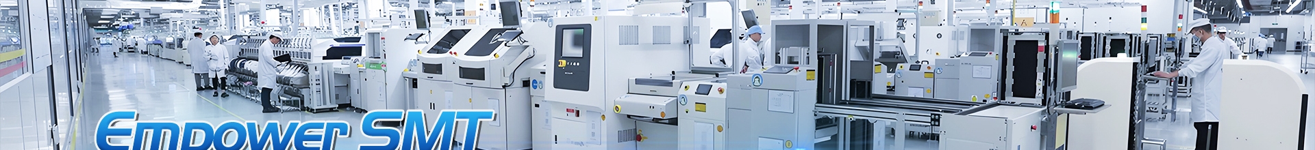
Now, speaking of companies leading the charge, MOREL EQUIPMENTS CO., LIMITED has been around for over 15 years, and they’ve really grown from just providing accessories to offering full-on solutions in this industry. Their commitment to staying on top of the game shows in their product range — stuff like advanced pick-and-place machines, automatic soldering robots, and automated testing equipment. All of these are designed to meet the crazy demanding needs of today’s PCB manufacturing. Pretty impressive, huh?

When it comes to designing and manufacturing electronic devices, PCB routing plays a huge role—it's pretty much the backbone of how all the components talk to each other. If you’re just getting started, it’s helpful to understand that good PCB routing is really about finding that sweet spot between making a design intricate enough to work well but still easy enough to manufacture without headaches. Interestingly, the IPC (that’s the Institute of Printed Circuits) points out that nearly 70% of PCB-related problems actually come down to inept routing techniques. That can cause everything from electrical hiccups to big delays and extra costs in production. So, yeah, having solid routing strategies is more important than ever these days.
Lately, things have really taken off thanks to advances in automation and smart software. Companies like Morel Equipments Co., Limited—who's been around for over 15 years in the SMT world—really get how crucial it is to adopt the newest tech in PCB making. With AI-powered design tools now a thing, manufacturers can route circuits more accurately and efficiently, cutting down on errors and making complex layouts way easier. In fact, reports say that switching to automated solutions can slash PCB assembly times by up to 40%. Not too shabby, right? As a full-service provider, Morel stays ahead of the game by focusing on innovations like high-speed pick-and-place machines and automatic soldering robots, making sure quality and productivity are always front and center in the industry.
In the realm of printed circuit board (PCB) manufacturing, optimizing processes is crucial for enhancing efficiency and achieving high-quality output. The CMQ360 Depaneling Router stands out as a revolutionary tool designed to meet these demands. One of its key advantages is the integration of a dual 16 million high-speed camera auxiliary programming system, which streamlines the programming process, making it more intuitive and efficient. This feature aligns with industry reports, such as those by IPC, which emphasize that automation and advanced imaging can significantly cut programming time by up to 30%.
Moreover, the CMQ360 is equipped with a high-speed CCD vision automatic correction system that greatly enhances cutting accuracy and operational efficiency. According to a recent market analysis, precision in PCB assembly and cutting operations is critical, with inaccuracies potentially resulting in losses up to 10% of total production costs. With the added capability of its high-speed spindle, the CMQ360 caters to a variety of board shapes, ensuring low splitting stress and high precision. This versatility is vital in an industry frequently shifting towards custom and specialized designs.
The dual-table movement feature of the CMQ360 further boosts productivity by allowing simultaneous processing of different products, thus minimizing downtime. Coupled with an external dust collection cabinet, designed for low noise and effective sealing, the router not only reduces operational costs through reusable integrated bags but also creates a cleaner working environment. Such innovations are essential in meeting the increasing demands for efficiency and sustainability in PCB manufacturing, reinforcing the CMQ360's position as a leading choice for manufacturers aiming to optimize their production processes.
: Recent trends in PCB routing technology include the integration of AI-driven design software and machine learning algorithms, which enable optimized routing paths that minimize signal interference and enhance performance.
The global PCB market is predicted to grow at a CAGR of 4.7%, reaching approximately $83 billion by 2025.
The integration of 5G technology and the Internet of Things (IoT) is significantly influencing PCB design methodologies, leading to a demand for advanced PCBs in IoT applications expected to grow by over 20% through 2024.
Signal integrity is crucial in PCB designs because over 70% of PCB failures can be attributed to signal integrity issues, making it essential for efficient and reliable performance.
Best practices for managing signal integrity include careful control of trace lengths, proper impedance matching, using differential signaling, implementing ground planes, and reducing the number of vias.
Simulation tools can predict how design changes affect signal performance, allowing engineers to optimize layouts before production, leading to improved performance and cost savings.
As the demand for more complex designs, such as multi-layer boards, increases, innovative PCB routing techniques are necessary to accommodate these complexities while maintaining efficiency and cost-effectiveness.
Maintaining a consistent reference ground decreases potential electromagnetic interference (EMI), which contributes to more robust signal integrity in PCB designs.
Effective PCB layout management ensures improved performance and reliability, ultimately leading to lower manufacturing costs and reduced time-to-market.
Future developments in PCB routing are likely to focus on creating smarter, more responsive electronics that cater to the demands of a digitally connected world, leveraging emerging technologies for enhanced performance.
Hey, did you get a chance to check out that article on 'Exploring the Future of PCB Routing Techniques and Technologies'? It really digs into the essentials of PCB routing, giving a pretty clear overview of the core principles. What’s fascinating is how it also points out the new and upcoming tech that’s likely to shape how PCB routing develops down the line. There’s a strong focus on making routing more efficient and performing better by leveraging some pretty advanced methods. They also shine a light on the latest CAD tools—showing how these innovations can make designing and routing PCBs way easier. Plus, they talk about best practices for keeping signal integrity intact, which is especially important when we're dealing with all these IoT devices. Routing strategies need to adapt constantly in that space, after all.
On the business side, Morel Equipments Co., Limited—who are kinda big players in surface mount technology—really get how vital good PCB routing is. They've been around for more than 15 years, offering everything from top-notch Pick And Place Machines to automatic soldering robots. These tools are pretty much the backbone of improving PCB design, routing, and manufacturing overall. Honestly, their solutions help boost efficiency and make the whole process smoother and more reliable.